top of page


Some of our facilities
@ Nanoscale Optics Lab
Our Lab
 Chemical PreparationGlovebox for batching and melting various glasses and semiconductors as sputtering targets, lenses and substrates |  Nanoscale FilmsPhysical vapour deposition (RF and DC sputtering and Thermal evaporation) and high throughput material discovery of phototunable, reconfigurable and nonlinear chalcogenides, various metals and transparent conductive oxides. |  Rapid prototypingModified FDM and Photo-resin 3D printers with <10µm Resolution. |
|---|---|---|
 Annealing and MeltingMelting, oxidation and annealing of various metals, glasses and semiconductors under a variety of atmospheres and pressures. Up to 1100 Celsius furnaces Hotplate up to 500 Celsius Vacuum, N2, Ar and O2 atmospheres |  Optical mapping MicroscopyOptical microscopy of various samples with high resolution spatial mapping. |  Nanoparticle DepositionSpincoat, spray or sonicate various nanoparticles onto free space and integrated devices |
 HPC and SimulationsDedicated Windows and Linux servers for various atomic and device level 2D and 3D multiphysics simulations. |  SpectrophotometeryInverted microspectrophotometers with integrated pulsed and CW laser excitation and electrical probes and SMU’s for mixed-mode device interrogation. | 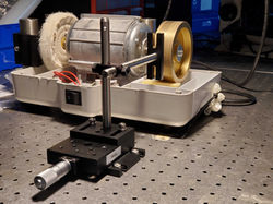 Glass PolishingOptical fiber cleaving, fusion splicing & glass polishing and cutting |
 Fiber integrated nanophotonic devicesMicrospectrophotometry with integrated laser excitation for the characterization of optical fiber integrated Nanophotonic devices. |  Glass sawCutting of substrates and small scale optomechanical components. |  Thermo-opticalUpright electro-thermo-optic microspectrophotometery with laser excitation and atmosphere controlled heating stage for environmental sensing applications |
 Hot PressHot press: We can manufacture sputtering targets ( up to 3” diameter) not available anywhere else. |  FumehoodFumehood for chemical storage and processing |  Probe stationElectrical and optical probing of devices. |
Nanofab
 Zeiss Sigma FESEM w/EDX&EBSDThe Sigma FESEM features the GEMINI column, which is optimized to operate at low kV imaging for excellent surface sensitivity. It is also configured with in-lens secondary electron (SE) detector and a backscatter (BSD) detector. The system also integrates the Oxford AZtecSynergy system with simultaneous EDS and EBSD acquisition which provides accurate phase identification and fast elemental/phase mapping. |  Heidelberg MLA150The MLA150 is a high-speed direct-write photolithography tool. Using laser light impinging on a digital micromirror array, the system exposes patterns from a CAD file directly onto photoresist-coated substrates, eliminating the need for a photomask, and resulting in a significantly shorter prototyping cycle. |  RAITH150 Two EBL SystemUltra-high-resolution, low-voltage (0.1–30 kV), electron-beam lithography tool, capable of writing structures over a 150 mm diameter wafer. |
|---|---|---|
 Nanoscribe Photonic Professional GTThe Nanoscribe Photonic Professional GT is the world’s highest-resolution 3D printer. Based on two-photon polymerization (2PP), it allows for additive manufacturing and maskless lithography with the same device. Submicron resolution printing with feature sizes down to 200 nm and optical quality surface finishes are characteristic key features. Two powerful writing modes move the laser focus with respect to the photoresist. |  LPCVDLow Pressure Chemical Vapour Deposition (LPCVD) of standard (stoichiometric) and low-stress silicon nitride and poly-Si. |  PECVDPlasma-enhanced chemical vapor deposition (PECVD) - This system is used for SiO2‚ and Si3N4 depositions. |
 Electron beam evaporationSix-pocket electron beam evaporation system with computer-controlled, automated deposition. Deposition materials are restricted to approved metals only. Pockets 1–5 are dedicated to aluminum, titanium, chromium, gold, and silver, respectively; pocket 6 may be switched at user request. |  ICPRIE (Oxford)A number of versatile, load-locked Inductive coupled plasma reactive ion etcher (ICPRIE) tools. |  Olympus Laser Confocal Microscope (OLS3000)3D imaging confocal microscope utilizing a 408 nm laser for fine surface non-contact profile measurements. |
 ICPRIE (AMS)A single-wafer load-locked DRIE system for deep etching of Si (Bosch) or glass substrates. Only photoresist or oxide may be used for etch masks (i.e., wafers cannot contain any exposed metal). |  He Ion Microscope with FIBThe Zeiss Orion NanoFab helium-ion microscope provides novel and unique microscopy and nanofabrication techniques. It enables high resolution imaging of insulating materials and devices with superb surface sensitivity and large depth of field. Ultra-high resolution fabrication can be achieved by direct patterning (material removal by sputtering) or lithography (resist exposure) with speed and ease. The system is also equipped with a Ga focused ion beam (FIB) column for massive material removal. |  Wire BonderSemi-automatic wire bonder with motorized Z- and Y-axes, used to create electrical interconnects between dies and packages/printed circuit boards. |
 Auger JEOL 9500FThe JAMP 9500F combines Auger electron spectroscopy (AES), ion sputtering and secondary electron imaging for determination of 2D and 3D elemental distributions on surfaces with high spatial resolution. This system can also provide depth profiling analysis. |  Alpha-Step IQ - W1-040Two-dimensional surface topography profiler with sub-8-Å step height repeatability and sub-Å resolution. Ideal for thin-film profilometry and measuring the step height of various materials. |  Ellipsometer (M-2000V)Variable-angle spectroscopic ellipsometer with 370-1000 nm wavelength range. |
 Four-Point Probe (Pro4 4000)Lucus Pro4 4000 sheet and bulk resistivity measurement system with Keithley 2601A sourcemeter, range: 1 mΩ to 100 MΩ per cm square. |  FTIR (Nicolet 8700)The Nicolet 8700 Fourier Transform Infrared (FTIR) Spectrometer 8700 is suited for analysis of bulk samples, thin films, powders and liquids. The available light sources include, infrared and white light with both polarized or non-polarized modes. Attenuated total reflection and specular reflectance operation modes are available. |  Atomic Force Microscope (Dimension Edge)Atomic force microscope |
 VASE EllipsometerThe Variable Angle Spectroscopic Ellipsometer is capable of high accuracy measurement of various optical properties of your thin films. |  Nanometrics Hall Measurement (HL5500)Semiconductor characterization of resistivity, carrier concentration and mobility utilizing the hall effect. |  TOF-SIMS Imaging Spectrometer (ION-TOF GmbH)Time of Flight-Secondary Ion Mass Spectroscopy (TOF-SIMS) is an ultra high sensitive surface analysis technique providing detailed elemental and molecular information about surfaces, thin layers and interfaces. |
 Rigaku XRD Ultima IVThe Rigaku Ultima IV is a state of the art, multipurpose X-ray (Cu-source) diffraction system. With cross beam optics (CBO) technology and automatic alignment capability, the Ultima IV is fast and flexible for a variety of applications including powder diffraction, thin film diffraction and in-plane scattering. This XRD has both parallel beam and focus beam slit, the detector is scintillation counter with monochromator. |  XPS Spectrometer (Kratos AXIS Ultra)The AXIS Ultra is a high sensitivity multi-technique photoelectron spectrometer capable of surface mapping to provide lateral distribution maps for elemental and chemical species at the surface. |  Profilometer (Tencor P-6)Contact surface profiler up to 150mm scan length without stitching. |
bottom of page